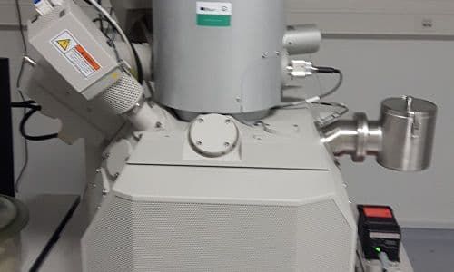
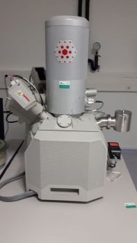
Scanning electron microscope with autoemission cathode
DEVICE IS FOR:
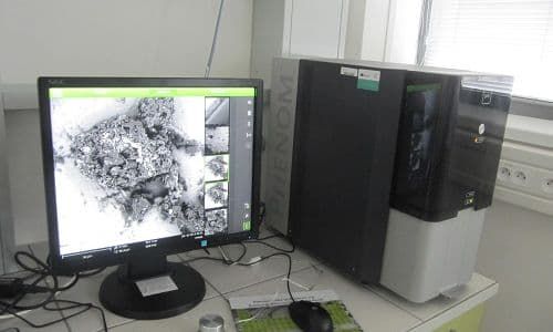
Scanning electron microscope Nova NanoSEM 450 (FEI) with Schottky field emission electron source operated at acceleration voltage ranging from 200 V to 30 kV. Combination of advanced optics including Through-lens SED (TLD), Everhart-Thornley SED, Low-vacuum SED (LVD), Through-lens BSED (TLD-B), Lens-mounted Annular GAD, Retractable DBS Detector, Retractable STEM 3, Retractable Energy dispersive X-ray (EDX) detectors and imaging modes delivers best-in-class imaging and analytical performance. Observation in following modes is available: • SEM – scanning electron microscopy using BSE a SE detectors, point resolution ≤ 1.0 nm at 15 kV, ≤ 1.4 nm at 1 kV, low vacuum mode ≤ 2 nm at 3 kV. • STEM – scanning transmission electron microscopy, point resolution ≤ 0.8 nm at 30 kV, with detectors for bright field, dark field, and high angle dark field imaging (Z contrast) • EDX – Energy dispersive X-ray spectrometry - TEAM EDS analysis system (EDAX) equipped with detector Octane plus (SDD, liquid nitrogen free), active area 30 mm2, Be window, Resolution at Mn Kα 129 eV and EDAX TEAM software The instrument contains active shielding against electromagnetic fields, cryogenic trapping system, plasma cleaning system for removal specimen contamination.
CONTACT:
IMAGING


