TEM microscope
DEVICE IS FOR:
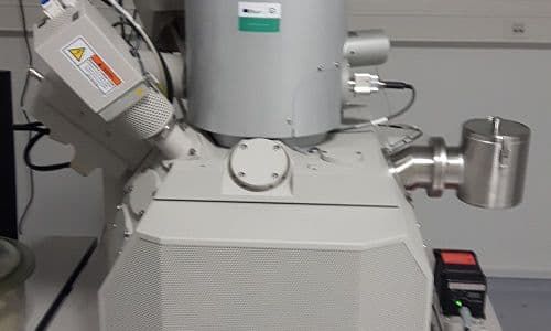
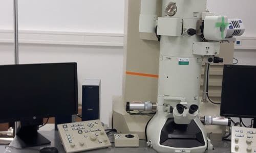
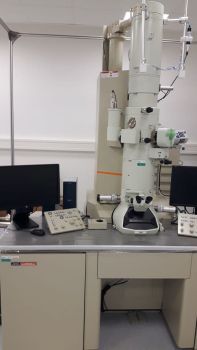
High resolution transmission electron micrscope JEOL JEM 2100 with high brightness LaB6 source operated at acceleration voltage ranging from 80 to 200 kV provides solutions for a wide range of problems in the fields of material science. CCD bottom mounted on-axis 14 bit camera OLYMPUS SYS TENGRA with resolution 2048 x 2048 pixels and exposition time ranging from 1 ms to 100 s enables high speed digital imaging with extraordinary resolution. Observation in following modes is available:
• TEM – Transmission electron microscopy (point resolution 0.23 nm, lattice resolution 0.14 nm).
• STEM – Scanning transmission electron microscopy with detectors for bright field and dark field imaging (Z contrast, point resolution ≤ 1 nm)
• EDX – Energy-dispersive X-ray spectrometry, AZtec TEM EDS system with X-Max 80 TEM analytical detector (SDD, liquid nitrogen free), active area 80 mm2, SATW Be window Resolution at Mn Kα 127 eV.
• NBD and CBD modes for crystalline structure analysis. The instrument contains automatic drift compensation system to avoid specimen moving, active shielding against electromagnetic fields, plasma cleaning system for removal specimen contamination, and switching option from TEM mode to STEM mode without focusing.
CONTACT:
IMAGING


